
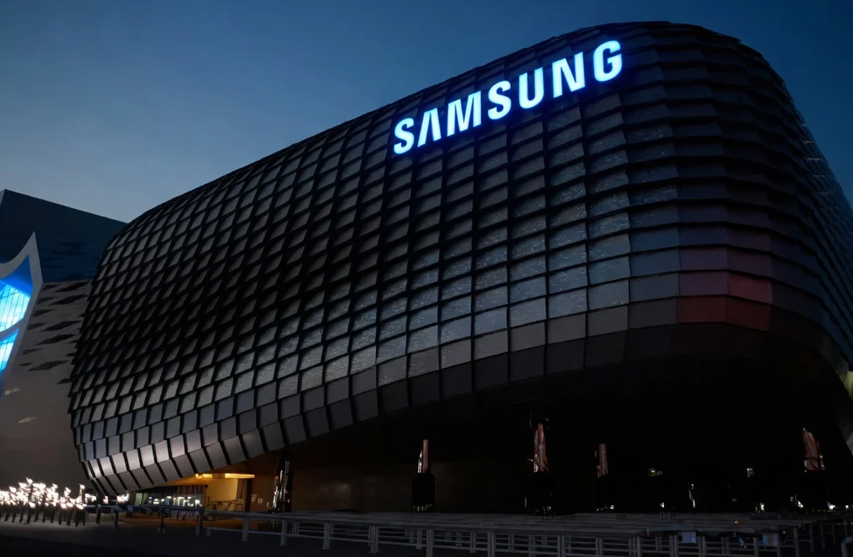
TSMC and Samsung, the two biggest chipmakers in the world, have agreed to use ASML's newest lithography machines. The tools are called High NA EUV machines. Demand for more advanced chips used in artificial intelligence is driving the move.
ASML's EUV machines print tiny circuit patterns onto silicon wafers. This step is a core part of making computer chips. The High NA version can print smaller and more detailed patterns than older models.
Each High NA machine costs around $400 million. That price makes it one of the most expensive tools in modern manufacturing.
Samsung and TSMC Adoption Plans
Samsung is one of the largest memory chipmakers in the world. The company said it will use ASML's High NA machines to produce DRAM, a common type of memory chip, starting in 2028.
Samsung said the move will extend its DRAM scaling roadmap. This means the company expects to keep improving memory chip performance for years to come.
TSMC said it plans to use the machines for advanced chip production by 2030. The company pointed to more complex transistor designs needed for AI applications as the reason.
TSMC said it expects use of High NA machines to grow over time. The company linked this growth directly to rising AI chip demand.
Investor Reaction and Next Steps
Investors have watched closely to see how many chipmakers would commit to the new machines. ASML stock has climbed 120% over the past year.
Analysts at Barclays said the announcements give more clarity on how widely the technology will be adopted. Barclays called this a positive development for ASML.
Despite the news, ASML shares were flat to lower in early trading Tuesday in Amsterdam. Stock moves do not always match the tone of company news.
Samsung and TSMC now join Intel as customers for the High NA machines. Intel began using the technology for advanced chip manufacturing in July.
ASML has not shared a public forecast for how many High NA machines it expects to sell. The company has said it will add about 30% more EUV production capacity by 2027.
Barclays said ASML faces a decision on whether to expand EUV capacity further. The firm said demand for the machines is clearly strong.
Samsung and TSMC will also join ASML in a separate industry effort. The project aims to develop larger photomasks used in chip production.
Photomasks work like stencils that print patterns onto wafers. The industry currently uses a 6 inch format.
The new initiative will move toward a 12 inch photomask format. ASML said the larger size can improve productivity and lower chipmaking costs.
The photomask project marks another step in the shift toward AI focused chip manufacturing. Samsung, TSMC and ASML are working together on the standard.